When we pick up our phones or turn on our computers, the semiconductor packaging is the invisible hero behind every electronic device we touch. This technical term essentially describes the process of protecting the chip and connecting it —— Without this, even the most advanced chips would not function as the electronic components we use daily. So, what exactly does semiconductor packaging do? How does it transform a wafer into a functional chip? Lets explore its birth process to understand this better.
01.
From wafer to chip: the whole process of packaging disassembly
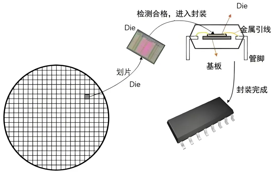
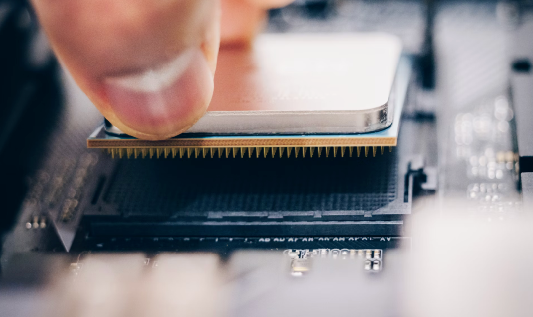
A complete wafer is like a chip puzzle, and the first step in packaging is to cut it into individual chips (Die). This process is similar to slicing a cake into smaller pieces, each of which becomes an independent integrated circuit. Next, these chip cakes are glued onto a substrate (similar to the frame of a circuit board), and then fine metal wires (such as gold or copper) are used to connect the solder joints on the chips to the pins on the substrate. This step involves building a wiring network for the chip, enabling it to communicate with the outside world.
After the circuit is connected, the chip needs to be encased in a protective shell. In the early days, the chip was fully sealed in metal tubes, but now it is more commonly wrapped in plastic to protect against dust and moisture that could damage its internal structure. However, packaging is not as simple as just putting on a shell: after being encapsulated with plastic, the chip must undergo processes such as post-curing, die formation, and electroplating. It then undergoes multiple rounds of testing, including simulations of high and low temperatures to ensure the chip functions properly. Only after passing these tests will the qualified chips be packaged and stored, ready to become the heart of electronic devices.
02.
The relay race of semiconductor manufacturing
Semiconductor production is akin to a relay race, where the front and back processes each play their part. The front process involves drawing circuits on the wafer, such as through photolithography and etching, among hundreds of steps, to etch nanoscale transistors and capacitors onto the silicon wafer. This step is like drawing a complex circuit diagram on a fingernail, requiring extremely high precision.
The packaging process, a post-processing step, takes over the semi-finished chips from the front-end and transforms them into functional chips. To put it another way: the front-end is like a designer, while the packaging process acts as an assembly engineer. It not only protects the chips but also ensures they can communicate with circuit boards and other components. Typically, these processes are carried out in separate factories, as the front-end requires an ultra-clean environment, whereas the back-end focuses more on assembly techniques.
03.
The "multiple identities" of packaging: protector & converter
Why do chips have to be packaged? Imagine that the circuits inside a chip are fine at the nanometer level, exposed like fragile glass and vulnerable to damage. The first role of packaging is to "protect" by shielding physical impacts and chemical corrosion with an outer shell.
However, more importantly, the package acts as the translator and connector for the chip. The pin spacing on a chip can be just a few micrometers, while the solder joints on a circuit board are millimeter-level. —— The package converts this small pitch to large pitch, allowing the chip to be easily soldered onto the circuit board, which is known as the size conversion function. Additionally, when the chip operates, it requires power supply and signal transmission. The packages pins and internal wiring act like a highway, ensuring that current and data flow smoothly.
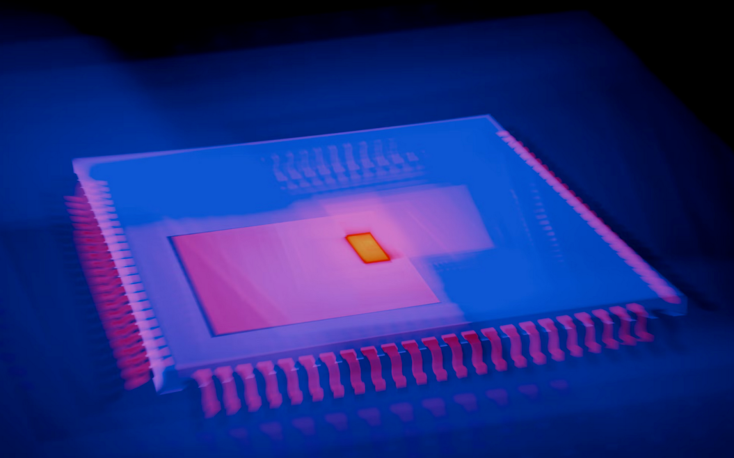
As chips get faster and faster, heat dissipation becomes a problem. The current package also has to act as a "heat sink", using material design to conduct the heat generated by the chip away from it and prevent it from "overheating" and breaking down.
04.
From chip to machine:
the "advanced road" of three layers of packaging
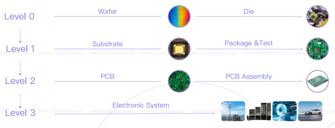
Encapsulation is not done in one step, it has a clear hierarchy:
Primary packaging: a single or multiple chips are "packaged" into a component, such as the processor chip in a mobile phone, which is fixed to the substrate by flip chip (Flip Chip) and then wrapped in plastic;
Secondary packaging: the first-level packaged chip is mounted on the circuit board (PCB), such as the computers graphics card, which is welded with multiple chips and components on the PCB;
Three-level packaging: assemble multiple circuit boards into a complete system, such as a computer host, which requires connecting components such as the motherboard, graphics card and hard disk to the chassis to achieve complete functions.
Its like building with blocks: the first level is a single part, the second level is a module, and the third level is a complete toy.
05.
The "evolutionary direction" of packaging technology:
smaller, faster and smarter
Today, as chips become smaller, their packaging is also becoming more compact. From the earliest DIP (Dual In-Pin Package) to todays BGA (Ball Grid Array) and CSP (Chip Scale Package), the size of these packages has been continuously reduced, while the number of pins has increased. For example, the BGA package of a mobile phone processor features hundreds of millimeter-sized solder balls densely packed on its bottom surface, resembling a honeycomb.
To make chips run faster, packaging technology has started to explore three-dimensional stacking techniques: stacking multiple chips like a stack of burgers, using vertical connections to reduce signal transmission distances. For example, 3D packaging of storage chips can pack more capacity into limited space. In the future, as heterogeneous integration technology advances, packaging could integrate different types of chips (such as processors, memory, and sensors) into a single package, making electronic devices more compact and intelligent.
When we talk about semiconductor packaging, we are essentially discussing how to bring chips from the lab to the real world. While it may not be as glamorous as chip design, it is a crucial link between technology and application. From a silicon wafer to a smartphone, packaging acts like a silent engineer, building protective walls and laying connection lines for the chip through a series of processes, ultimately making technology accessible to us.
06.
AlphaPro Chemical:
Using material technology
to "tailor" chip packaging
In the whole process of chip packaging, the choice of materials directly determines the reliability and performance of the packaging. AlphaPro specializes in semiconductor packaging materials, providing "customized protection solutions" for chips from three core application directions, and building a barrier for the stable operation of chips with professional products:
🔖
Edgebond corner binding scheme: give the chip a "cushion corner" protection
The edges of chips, like the sharp edges of precision instruments, are highly susceptible to damage from collisions during transportation or assembly. AlphaPro's Edgebond solution (edge bonding) creates a robust protective edge by applying and curing a specialized adhesive around the chip. The companys core products, 5828 and 5105, are both one-component epoxy resin-based thermosetting materials, effectively providing a crash-resistant guard for the chip:
☑︎ Excellent bonding: firmly attached to the edge of the chip and substrate, resist external impact;
☑︎ Thermosetting molding: after heating, it is cured into a tough shell, which is not easy to crack and fall off in long-term use;
☑︎ Compatibility: suitable for a variety of chip sizes and packaging processes, especially suitable for edge protection of high frequency and high speed chips.
🔖
Underfill bottom fill scheme:
the solidification technique to lay the foundation for the chip
The tiny gap between the chip and the substrate, akin to a crack in a building foundation, can lead to connection failure due to thermal expansion and contraction. AlphaPro’s Underfill solution (bottom filling) addresses this issue by injecting adhesive into the gap at the bottom of the chip, creating a uniform support layer. Both products 5101 and 5101B use a one-component epoxy resin thermosetting system:
☑︎Fill and reinforce: fill the gap between the chip and the substrate, disperse the stress, prevent the weld from cracking;
☑︎Low viscosity penetration: glue can quickly penetrate to the micron level gap, adapt to high density packaging requirements;
☑︎Thermal stability: the low coefficient of expansion is maintained after curing, and it can work stably in the environment of-40℃~150℃ to ensure the long-term reliable operation of the chip.
🔖
The bond bonding scheme: the "golden link" connecting the chip to the substrate
The bonding process is like the "foundation" of chip packaging, which requires materials with both strong adhesion and conductive properties. The representative product of AlphaPro, 8392 bonding adhesive, has become the core material for packaging connection with its "all-purpose" characteristics:
☑︎Dual performance guarantee: both excellent bonding strength and conductive ability, volume resistivity as low as 10-⁴Ω·cm level, to ensure smooth current transmission;
☑︎High efficiency production adaptation: meet the high UPH (hourly capacity) demand, can quickly glue curing, improve the efficiency of the production line;
☑︎Heat dissipation and reliability: The low thermal impedance design accelerates chip heat dissipation, avoids high temperature failure, and is compatible with a number of industry certifications (such as UL, MSL levels), suitable for automotive electronics, 5G communication and other high-demand scenarios.
Summary:
In the precision world of semiconductor packaging, every product from AlphaPro serves as a hard-core solution for protecting chips. If you have more questions about packaging material solutions or want to know how our products can fit your specific application scenarios, feel free to leave comments in the comment section or contact us via the backend to get customized solutions——We look forward to exploring more possibilities in chip protection with you.