
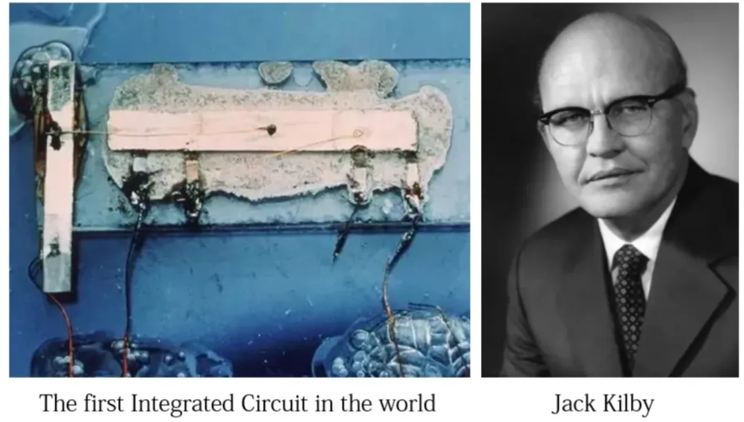
In 1958, the worlds first integrated circuit (IC) was born. Over the following six decades, the semiconductor industry experienced rapid growth, profoundly reshaping human lifestyles. Today, semiconductor products centered around integrated circuits have been widely integrated into various application fields, forming a solid foundation for the information age. Killebrew was awarded the 2000 Nobel Prize in Physics for his outstanding contributions.
In recent years, the price of a single ASML lithography machine in the Netherlands has exceeded $100 million. Alibaba established "Pingtouge" semiconductor companies, SoftBank spent $31 billion to acquire ARM, and China set up a large integrated circuit fund exceeding 130 billion yuan to boost industry development. Meanwhile, U.S. sanctions on ZTE and the Wassenaar Arrangements restrictions on exports of advanced technologies and products to China have led to Chinas integrated circuit imports surpassing crude oil imports for many years. Coupled with the Huawei incident and the Sino-U.S. trade disputes, these events have made people clearly recognize the critical value of semiconductors and the relatively lagging status of China in this field.
Semiconductor chip manufacturing process is highly complex, which can be roughly divided into wafer manufacturing, chip manufacturing, packaging and testing, etc. The complete process from raw material purification to finished product packaging can reach more than a thousand steps.
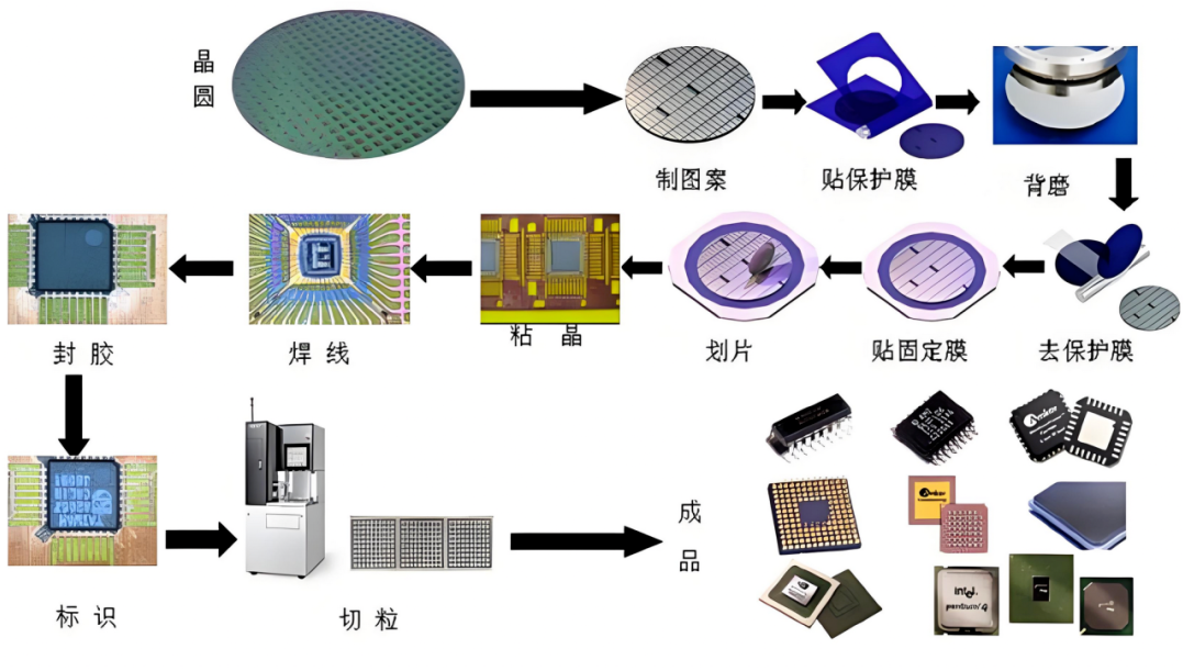
Wafer manufacturing process: mainly involves purification, crystal pulling, slicing, polishing and other technical processes
Chip manufacturing: mainly covers photoresist coating/removal, exposure, etching, ion implantation, physical/chemical vapor deposition and other technical operations, as well as grinding, cutting and other back-end processes
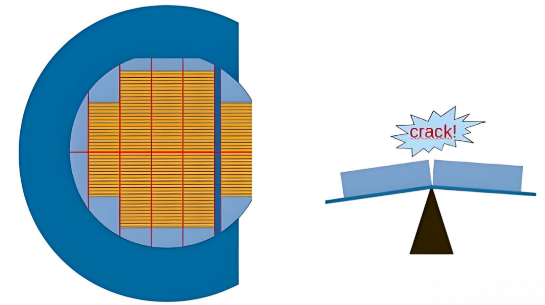
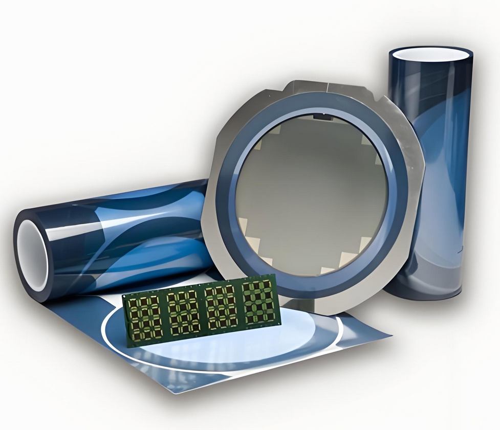
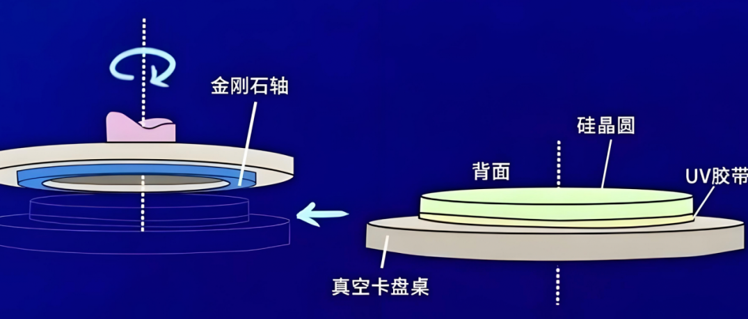
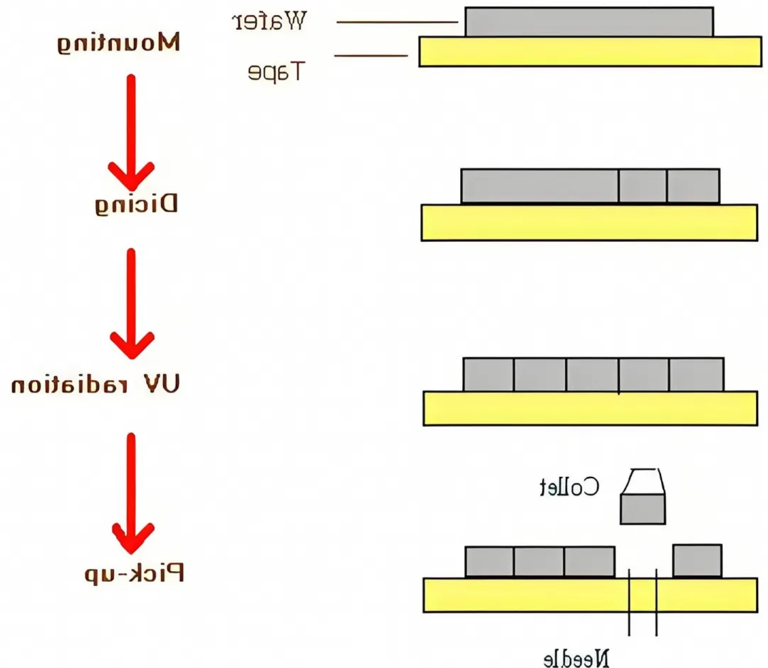
In the back-end processes of chip manufacturing, grinding and cutting require the use of grinding and cutting tapes. Given that silicon wafers are hard and brittle, they are prone to breakage due to stress during this process, especially in the backside grinding and cutting stages where fractures are more common. Therefore, protective tapes have become an indispensable consumable, with a global market size of approximately 13 billion RMB.
So, in the actual production process, what protection solutions are there?
The following is a high cost-performance solution led by AlphaPro's team of overseas experts who have worked for many years in international enterprises and laboratories in EU, US, JP and other countries, and they returned to China with mature experience.
01
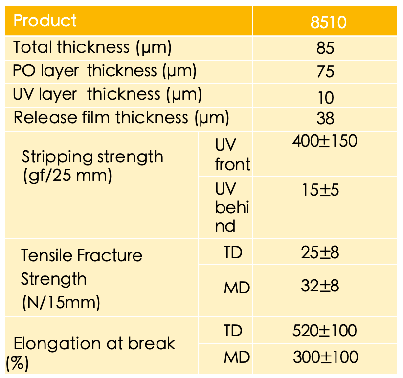
Backside grinding protection tape —— BG TAPE
l Function:
Applied to the front of the wafer (with circuit area), in the grinding and thinning process, protect the chip circuit from foreign damage, effectively prevent cracking, cracks and dirt problems.
l Market demand:
The global annual demand exceeds 12 million square meters.
l Qualification:
1. High adhesion to ensure that the chip is firmly attached and prevents displacement or detachment;
2. Under certain conditions (hot water bath or UV irradiation), the adhesion decreases rapidly;
3. Low pollution, no glue residue.
02
UV curable DICING TAPE
lFunction: During cutting, the crystal chip is firmly attached with super adhesion to ensure that the small crystal chip does not move, prevent the crystal chip from falling off and scattering during cutting, and ensure the smooth cutting.
lMarket demand: the annual global demand exceeds 20 million square meters.
lQualification:
1.The cutting has high adhesion and high followability to the chip;
2.Under certain conditions (hot water bath or UV irradiation), adhesion decreases rapidly;
3.Low pollution, no glue residue.
03
QFN. Packaging Tape
At present, there are many chip packaging methods, even close to 100 kinds, among which a very popular way is called QFN packaging, Quad Flat No-leads Package, square flat pinless packaging.
QFN Packaging Progress
In this process, a single-sided tape is used, with the base material being PI polyimide and the adhesive being acrylic. The specific steps are as follows: attach the QFN tape to the back of the lead frame, then apply conductive or insulating adhesive. After it cures, gold wires are attached to each pad on the conductor. Subsequently, epoxy resin is used for potting. Once the encapsulation is complete, remove the tape. This tape must leverage the high-temperature resistance of PI to meet process requirements. Additionally, silicone cannot be used as an adhesive because it can cause silicon contamination. Acrylic adhesives also present challenges in meeting high-temperature resistance requirements and must ensure no residual adhesive remains after use.
The most popular domestic alternative product of AlphaPro at present - 7281, uses high-temperature resistant PI substrate, precisely cut by imported Japanese equipment to ensure no burrs or fringes; meanwhile, it is free of adhesive during use, easy to peel off without leaving any adhesive residue; it is highly suitable for use before wire bonding.
04
Chip adhesive film
DA FILM
There are a variety of materials available when the chip is fixed to the lead frame or bonded to two layers of wafers. Adhesive (die attach adhesive) can be used, or thermosensitive DAF film (Die attach film) can be selected, or CDAF material with
Designed with low modulus and high flexibility, it can better relieve stress and reduce the risk of chip damage. In terms of cost, compared with traditional die attach adhesives, using AlphaPro's DAF can save 50-60% of the cost. It is widely applicable to multiple fields such as smartphones, computers, automotive electronics, and Internet of Things devices, and can easily achieve advanced packaging that is thinner and has a higher density.
Adhesive Technology
l Adhesive technology Adhesive technology is very comprehensive, which can be evaluated from the following four dimensions:
1. Design and synthesis of adhesives and resins: In-depth professional knowledge and rich practical experience are required to accurately control the properties and reactions of chemical substances, so as to develop adhesives and resin components with specific properties to meet the bonding requirements of tapes in different application scenarios.
2. Resin modification and dispersion ratio: Through the modification of resin and precise adjustment of its proportion in adhesive, the overall performance of adhesive is optimized, such as bonding strength, temperature resistance, chemical resistance, etc., so as to adapt to complex and changeable use conditions.
3. Application Development: Conduct detailed application research and development for specific products and their particular scenarios. This requires a deep understanding of the material, surface characteristics, and usage environment of the adhesive to tailor the most suitable adhesive solution, ensuring that the tape performs stably and reliably in practical use.
4. Precision Coating Technology: The adhesive is applied uniformly and accurately onto the substrate, ensuring that the absolute thickness meets stringent standards while keeping tolerances within an extremely small range to guarantee uniformity. This process requires high-precision coating equipment and sophisticated process control techniques; any minor deviation in coating can affect the final performance of the tape.
Engineering Technology
Customized Design: Due to the differences in processes among semiconductor manufacturers, the performance requirements for substrates vary as well. Therefore, it is necessary to design and provide multiple substrate products tailored to specific customer needs. However, AlphaPro have strong R&D capabilities and a diverse product line, enabling to quickly respond to market changes and customer demands, offering personalized solutions.
In the face of these technical challenges, AlphaPro has recently achieved a breakthrough in mass production with more than 15 years of experience. The following are the relevant existing product application scenarios. Please leave a message to contact us for samples.